
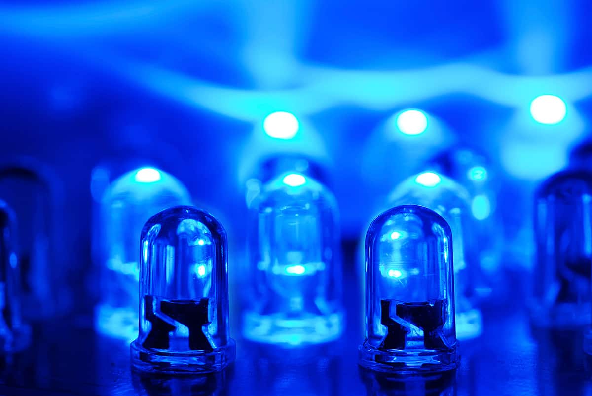
Because blue light emission requires special material qualities and manufacturing technology, the creation of blue LEDs presented enormous problems that took decades to overcome. According to BBC News, researchers Isamu Akasaki, Hiroshi Amano, and Shuji Nakamura didn’t make the breakthrough until the early 1990s, which changed lighting technology and earned them a Nobel Prize in Physics.
Shuji Nakamura’s Significant Development
Three Japanese scientists—Isamu Akasaki, Hiroshi Amano, and Shuji Nakamura—are credited with creating the blue LED. Researchers had been unable to create effective blue light-emitting diodes for decades before their pioneering work in the early 1990s. This accomplishment’s importance in the field of optoelectronics was highlighted by the 2014 Nobel Prize in Physics.
In particular, Shuji Nakamura was instrumental in bringing blue LED technology to market. Even though Nakamura was initially only given a meager bonus of ¥20,000 (about $180) for his innovation while he was employed at Nichia Corporation, his perseverance and creativity were crucial in overcoming the technological obstacles that had long impeded the development of blue LEDs. His research, together with those of Akasaki and Amano, transformed lighting technology and opened the door for the development of white LEDs, which resulted in more ecologically friendly and energy-efficient lighting options all over the world56.
Material Difficulties With Blue LEDs
Because of the particular semiconductor characteristics needed for blue light emission, the creation of blue LEDs brought with it special material problems not seen in red and green LEDs. It took years of research to solve the major challenges presented by gallium nitride (GaN), the essential component for blue LEDs.
Finding an appropriate substrate for producing high-quality GaN crystals was one of the main obstacles. GaN did not fit possible substrates like sapphire or silicon carbide (SiC) well in terms of atomic lattice spacing, in contrast to other semiconductors utilized in LEDs. The GaN crystal structure developed a high density of defects as a result of this mismatch, drastically lowering the LEDs’ lifespan and efficiency.
Achieving effective p-type doping in GaN was another significant challenge. The creation of p-type GaN was quite challenging, but n-type doping was rather simple. Finding appropriate acceptor dopants that could induce holes in the material was difficult due of GaN’s large bandgap, which is required for blue light emission. GaN’s propensity to produce nitrogen vacancies, which serve as inadvertent n-type dopants and offset any p-type doping attempts, made this problem worse.
In addition, GaN’s large bandgap made carrier injection and recombination difficult. It was challenging to effectively inject carriers into the LED’s active region due to the high energy barrier separating the p-type and n-type regions. Furthermore, keeping the injected electrons and holes from mixing in undesirable ways was essential to attaining high efficiency, particularly considering the wide band gap needed for the emission of blue light.
To overcome these material obstacles, researchers had to create novel methods. For example, buffer layers were used to reduce defect density4 by mitigating the lattice mismatch between GaN and the substrate. The finding that magnesium-doped GaN could be activated by low-energy electron beam irradiation or thermal annealing, which eliminated hydrogen passivation of the magnesium acceptors, marked a breakthrough in p-type doping.
Compared to its red and green siblings, blue LEDs took a lot longer to develop, which can be explained by these material issues. In order to overcome these challenges, advancements in growing methods, device design, and material science were all necessary, which finally resulted in the ground-breaking blue LED technology of today.
Developments In LED Manufacturing Technology
Significant improvements in manufacturing processes, especially in metal-organic chemical vapor deposition (MOCVD), were necessary for the creation of blue LEDs. To produce high-quality GaN crystals with few flaws, this procedure needed to be improved. In order to increase production and boost LED efficiency, innovations like buffer layers and better reactor designs were essential. Furthermore, improved electron and hole confinement made possible by the addition of quantum wells and heterostructures to the LED design greatly increased light output and recombination efficiency. The “blue LED problem” that had held up LED technology for decades was resolved thanks in large part to these technological advancements.
Blue LED Technology’s Effect
The invention of blue LEDs has had a significant influence on daily life and technology. Blue LEDs revolutionized lighting and display technologies by completing the trio of primary hues along with red and green LEDs. This allowed for the development of full-color screens and white light sources.
Energy-efficient lighting has been one of the biggest effects of blue LED technology. Since they have longer lifespans and use a lot less energy than conventional lighting technologies, white LEDs—which are made by mixing blue LEDs with yellow phosphors—have emerged as a key component of contemporary lighting systems. This innovation has been widely used in a variety of applications, such as street lamps and home illumination, supporting international initiatives to conserve energy and lower carbon emissions. Furthermore, the creation of brighter, more colorful, and energy-efficient screens for televisions, cellphones, and other electronic devices has been made possible by blue LEDs, which have been essential in the advancement of display technologies.