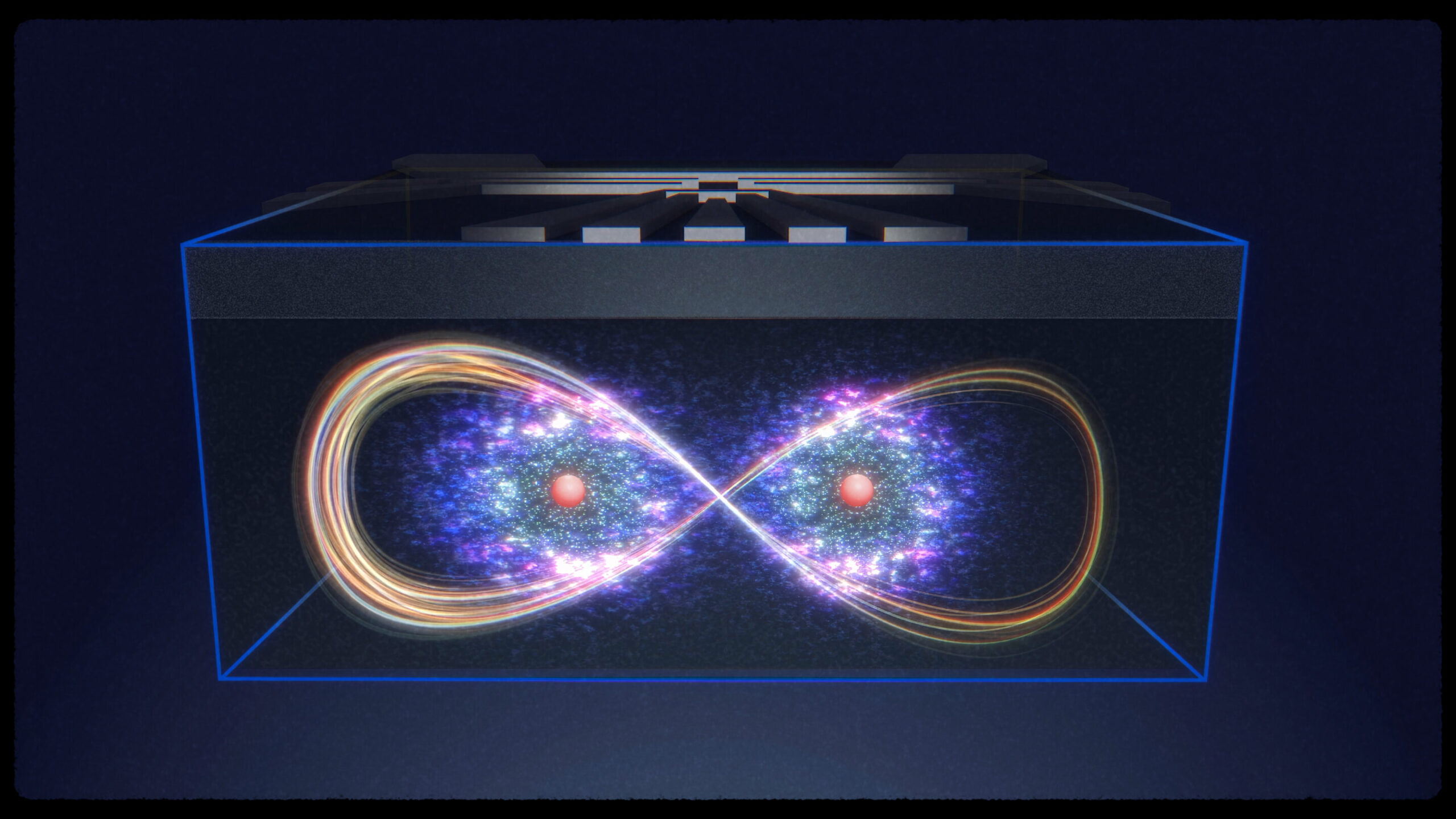
By employing electrons as bridges to allow for long-distance communication between quantum particles, engineers at the University of New South Wales have successfully created quantum entanglement between atomic nuclei that are 20 nanometers apart. By resolving the fundamental problem of sustaining quantum connections at chip manufacturing scales, the discovery—which was published on September 18 in the journal Science—showcases a workable strategy for scaling up quantum computers.
Under the direction of Dr. Holly Stemp and Professor Andrea Morello of Scientia, the research team was able to successfully construct “quantum entangled states” between the nuclei of phosphorus atoms implanted in silicon chips. By using distinct electrons that may “touch” one another over long distances, this technology enables nuclei to communicate, in contrast to earlier approaches that required atomic nuclei to share a single electron.
Significant Advancement In Quantum Computing Based On Silicon
A fundamental engineering issue in quantum computing was overcome by the UNSW team: striking a balance between allowing quantum particles to interact for meaningful computation and ensuring insulation from outside noise. Their method uses phosphorus atoms’ nuclear spins as qubits, which have an error rate of less than 1% and can retain quantum information for more than 30 seconds.
“We succeeded in making the cleanest, most isolated quantum objects talk to each other, at the scale at which standard silicon electronic devices are currently fabricated,” Stemp said. Integration with current semiconductor manufacturing methods is made possible by the 20-nanometer separation, which is comparable in size to contemporary silicon transistors found in computers and smartphones.
AI Quickens The Discovery Of Materials
At the same time, scientists at Oak Ridge National Laboratory created a Bayesian deep learning-based AI technique for examining atomic structures and their quantum characteristics. According to Ganesh Narasimha of ORNL, the method automatically finds areas of materials with intriguing quantum characteristics, significantly cutting down on experimental time.
The AI method effectively investigates materials such as europium zinc arsenide, a magnetic semimetal with distinctive electrical characteristics, by fusing probability theory and neural networks. The creation of novel quantum materials for a range of applications may be accelerated by this expedited discovery process.
Microsoft Increases Its Quantum Infrastructure
Early access to Microsoft’s experimental Majorana 1 quantum chip will be provided as part of the company’s plans to establish a new quantum research center at the University of Maryland’s Discovery District. The facility is part of Maryland’s $52.5 million “Capital of Quantum” effort, which will give government agencies, researchers, and businesses access to state-of-the-art quantum gear.
“Maryland is placing significant wagers on the future in an effort to stimulate innovation and expand our economy. “The core of that strategy is quantum,” said Governor Wes Moore of Maryland. With possible access to up to $100 million in matching federal funds through collaborations with the Defense Advanced Research Projects Agency, the center seeks to bring together federal and state quantum leadership in the Washington, D.C., area.
As the area moves from experimental notions to commercially viable technology, these advancements mark a huge step forward toward real-world quantum computing applications, ranging from medicine discovery to climate prediction.

